
The abbreviation "CCD" stands for "charge-coupled device," referring to an electronic component designed specifically to move electrical charges from one location to another. Originally conceived in 1969 at Bell Laboratories by Willard Boyle and George E. Smith, this technology was initially intended as a means of data storage. While it never caught on for that purpose, its ability to convert light into electronic signals proved transformative for imaging.
CCD sensors work by leveraging the "inner photon effect" — exposing a semiconductor material to light causes charges to build up, and those charges are then shifted step by step through vertical and horizontal registers toward a central analog-to-digital converter. Think of it like a bucket brigade, where each bucket passes its contents along until it reaches the end of the line. The movement of charge is driven by carefully timed voltage pulses applied to a series of electrodes.
How a Charge-Coupled Device Works
Charge transfer mechanism inside a CCD
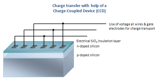
Voltages applied to the electrodes (-5V, -5V, +5V) shift negative electrical charges created by light exposure through the sensor one step at a time.
Did you know? Willard Boyle and George E. Smith were awarded the Nobel Prize in Physics in 2009 — exactly 40 years after their groundbreaking discovery of the CCD principle. Their work laid the foundation for modern digital imaging.
An image sensor that relies on this charge-shifting method to read out pixel data is known as a "CCD sensor." The speed at which the sensor can move charge from one pixel to the next is referred to as the "pixel clock." Traditional CCD sensors operated at pixel clock frequencies ranging from 25 to 50 MHz.
How CCD Sensors Respond to Light
A simplified look at the photoelectric principle
At the heart of every CCD sensor is the inner photoelectric effect. Within the silicon crystal structure, atoms have electrons distributed across different energy levels — a lower "valence band" and a higher "conduction band." Under normal conditions, most electrons sit in the valence band. However, when energy from outside sources (such as light) is introduced, electrons can jump to the conduction band, becoming free to move.
This transition requires a minimum of approximately 1.26 electron volts (eV). In a CCD sensor, that energy typically comes from incoming photons of light — though it can also be generated by heat within the sensor itself, which is known as "dark noise." Notably, 1.26 eV corresponds roughly to infrared radiation at a wavelength of about 1 µm. Light with longer wavelengths simply passes through silicon without being absorbed, which is why silicon-based sensors are essentially transparent to those frequencies.
When a photon strikes the silicon and excites an electron, it leaves behind a positively charged "hole." These freed electrons and holes separate due to the voltage applied across the sensor and are stored within individual memory cells rather than flowing immediately to the outside (as they would in a CMOS photodiode). The accumulated charge is then transported through the sensor in small steps toward a centralized amplifier and analog-to-digital converter.
Common CCD Sensor Configurations
Understanding the three primary layout types
CCD sensors generally come in three major architectural variants: the interline transfer CCD, the full frame transfer CCD, and the frame transfer CCD. Among these, the interline transfer design became the dominant choice in machine vision applications due to its support for electronic shuttering and fast frame rates.
Interline Transfer CCD Sensor
The most widely adopted CCD layout in industrial machine vision
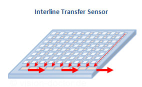
The interline transfer sensor arrangement showing light-sensitive pixel columns alternating with shielded transfer registers.
The interline transfer design was the only architecture capable of achieving very fast frame rates thanks to its built-in "electronic shutter" capability. For this reason, it was employed in roughly 90% of all CCD-based industrial machine vision cameras up until around 2015. After that point, improved CMOS sensors — particularly from manufacturers like Sony and ON Semiconductor — began to match and surpass CCD image quality, leading to the gradual discontinuation of CCD product lines.
Frame transfer CCDs and full frame transfer CCDs, on the other hand, found their niche primarily in scientific imaging. These architectures were preferred in situations requiring extremely low image refresh rates where maximum light sensitivity was the priority.
CCD Technology: Strengths & Limitations
Why CCD once dominated — and why CMOS took over
Because every pixel's charge is funneled through a single central amplifier and A/D converter, CCD sensors offered several notable advantages over early CMOS technology. However, the CCD approach also came with inherent drawbacks. Today, CCD technology is considered obsolete for mass-market applications, as modern CMOS manufacturing — driven heavily by the smartphone industry — has advanced to the point where CMOS sensors outperform CCDs in nearly every metric.
✓ Historical Advantages of CCD
Greater sensitivity & lower noise — thanks to a higher fill factor and enhanced surface utilization
Fewer defective pixels — a result of the simpler overall sensor architecture
Superior image uniformity — because all pixels share the same central A/D converter
✗ Persistent Disadvantages of CCD
Slower readout speed — limited by the single centralized A/D converter
No direct pixel access — data must be read out sequentially, unlike CMOS sensors
Larger & more expensive cameras — additional circuitry increases size and cost
Higher power consumption — the entire camera system draws more energy
Smearing & blooming artifacts — overexposure causes more visible distortion compared to CMOS
Since roughly 2015, advances in CMOS manufacturing have allowed CMOS sensors to surpass CCD image quality across the board. As a result, virtually all camera manufacturers have transitioned their product lines to CMOS-based systems. The CCD sensor, while historically significant, is now effectively retired from mainstream production.
Experience Classic CCD Imaging
The Leica M9 remains one of the most celebrated cameras to feature a full-frame CCD sensor — capturing images with a character and richness that digital photographers still seek out today.
Leica M9 Black© Backyard Provider • Your Trusted Source for Quality Equipment & Outdoor Living